[ Instrument R & D in Instrument Network ] Silicon chips are the core of contemporary information technology, and are currently developing in two directions: "More Moore" and "More than Moore." The Internet of Things (IoT) application is a very important part of the "Beyond Moore" technology route. It requires a large number of integrated circuit chips to analyze and process massive signals from external sensor devices. At present, most sensor signal acquisition devices and signal processing units are designed separately, which will generate greater power consumption and occupy more space as a whole.
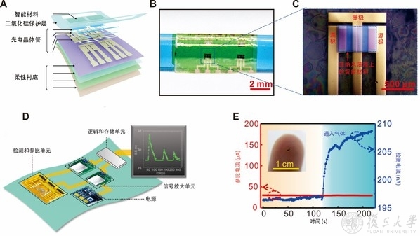
Figure 1: (A) Schematic diagram of the main functional layers of the device; (B) flexible sensor device array attached to the curved surface; (C) optical micrograph of the functional area of ​​the smart sensor device; (D) integration for humidity sensing System structure diagram; (E) The current changes of the reference device and the detection device before and after the introduction of hydrogen. Red is the reference current, and blue is the detection current.
As a result, Mei Yongfeng, a professor from the Department of Materials Science at Fudan University, proposed a new concept of integrating signal detection and analysis functions into the same chip device. As a demonstration, the research team combined and assembled single-crystal silicon thin-film flexible phototransistors with smart thin-film materials to construct a flexible silicon chip sensor and its system for detecting and analyzing different environmental variables. This idea is not only excellent in scalability, but also compatible with the current advanced manufacturing process of integrated circuits.
On May 2, the relevant research results were published in "Science Progress" ("Silicon Nanomembrane Phototransistor Flipped with Multifunctional Sensors towards Smart Digital Dust") Science Advances). The research team started with the sensing mechanism of the device and assembled an integrated chip sensor using a flexible thin film to realize the integration of various environmental parameter detection functions.
Smart materials can undergo changes in optical properties such as refractive index, color, and crystal structure during environmental stimulation, but generally require spectroscopic equipment or color charts for comparison. The flipped silicon thin-film phototransistor can easily obtain highly sensitive sensing characteristics because there is no light signal absorption in the gate metal barrier function area. Using this point, the research team attached a variety of smart thin film materials to the device functional area. The changes in the physical properties of the smart materials caused small optical performance changes, which were reflected in the output photocurrent, so the same chip Simultaneous detection of multiple different signals.
Figure 1A shows a typical functional layer structure of a sensor device. The smart thin film material on the top layer responds to environmental stimuli, thereby changing the output signal of the silicon single crystal thin film phototransistor below. The thermally oxidized silicon dioxide layer with a thickness of 2 microns is used as a phototransistor package to protect the underlying devices. The silicon thin-film phototransistor is completely prepared by wafer-level advanced integrated circuit technology, combining the high performance of traditional silicon-based optoelectronic devices with the excellent flexibility of ultra-thin silicon nano-film thickness. Figure 1B is a flexible device array attached to a glass tube with a radius of only 2 mm in diameter, showing good bending performance. Figure 1C is a close-up of the functional area of ​​a single device. Different intelligent materials can be integrated in the blue virtual frame to detect different environmental signals. Figure 1D is a composite diagram of a flexible system with complete sensing and data processing functions, including sensing and reference devices, logic and storage units, signal amplifiers, and power supplies. The research team used the system to achieve real-time and rapid detection of humidity in the environment, and the demo signal was three humidity pulses that were sequentially reduced. The signal that directly responds to environmental changes during the entire process, that is, the output current of the reference device and the sensor device changes with time as shown in FIG. 1E. When the environment changes (hydrogen is introduced as shown in the figure), the output current of the sensor device greatly increases, while the reference current remains stable, and then processed by the differential circuit, the value of the detected environmental parameter can be given.
The research team has developed a novel sensing mechanism that combines smart materials with photoelectric sensing, and integrated the sensing module with subsequent signal processing modules to demonstrate its detection of various environmental parameters such as gas concentration, humidity, temperature, etc. The ability has already initially taken shape in the future of "smart digital dust." This strategy can also be applied to other digital sensing systems, and will have huge application potential in the post-Moore era.
The thesis was mainly completed by Dr. Li Gongjin, Ph.D. students Zhe Ma and You Chunyu, and was supported by the cooperation of Professor Taeyoon Lee of Yonsei University in Korea and Researcher Di Zengfeng of Institute of Microsystems, Chinese Academy of Sciences. This work was strongly supported by the National Natural Science Foundation of China, the Shanghai Science and Technology Commission, Fudan University, and the State Key Laboratory of Special Integrated Circuits and Systems.
Genuine Synchronizer Ring OEM, Genuine Synchronizer Ring, Santana Synchronizer Inner Ring, 1988 Santana Synchronizer Ring
ShaoXing Change Auto Synchronizer Ring Co.,Ltd , https://www.sxcjautoparts.com