Abstract: Direct digital frequency synthesis (DDS) technology is the third generation of frequency synthesis technology that has been rapidly developed with the development of digital integrated circuits and microelectronics technology after direct frequency synthesis and indirect frequency synthesis. DDS technology has the advantages of wide bandwidth, short frequency conversion time and high frequency resolution. The output phase is continuous, and the frequency, phase and amplitude can be programmed. It is often used for high-precision frequency synthesis and arbitrary signal generation. In the design of the engine electronic control unit (ECU) hardware-in-the-loop simulation system, this article uses the TMS320LF2407A to control two AD9852s to generate two synchronized arbitrary signals to simulate the real signal of the engine during operation.
1. Introduction of AD9852 and TMS320LF2407A AD9852 is a new type of direct digital frequency synthesizer produced by Analog Devices, USA. It features fast frequency conversion, high spectrum purity, wide operating temperature range, and high integration. The operating voltage is 3.3V, and there are 4 to 20 times programmable clock multiplication circuits on the chip. The maximum clock of the system can reach 300MHz, the output frequency can reach 120MHz, and the frequency conversion speed is less than 1μs. Internal 12-bit D/A converter, 48-bit programmable frequency register and 14-bit programmable phase register, with 12-bit amplitude tuning function, can generate high-stability analog signals with programmable frequency, phase and amplitude control.
TMS320LF2407A is a fixed-point DSP controller introduced by TI. It uses high-performance static CMOS technology to reduce the power supply voltage to 3.3V, reducing the power consumption of the controller. The shortest instruction is 25ns, which has strong real-time control capability. On-chip 32kB FLASH program memory, 2.5kB RAM, 500ns conversion time A/D converter, on-chip event manager provides PWM interface and I/O functions to meet various motor control requirements. On-chip SPI, SCI and CAN controllers are also integrated.
2. TMS320LF2407A and AD9852 hardware interface circuit In this system, the function of TMS320LF2407A is to calculate the waveform parameters of the signal to be generated, and send the control word to the internal control register of AD9852 to realize the programmable arbitrary signal. There are serial and parallel data transmission methods. The maximum serial transmission rate is 10 MHz, and the maximum parallel transmission rate is 100 MHz. In order to save DSP resources, on the premise of satisfying the system requirement, adopt the serial connection way, control the AD9852 with the on-chip serial peripheral interface (SPI) of TMSLF2407A. The block diagram of the interface circuit is shown in Figure 1.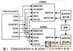
3. Serial communication work process of AD9852 The serial interface of AD9852 is compatible with the SPI interface of TMS320LF2407A. The serial data transmission control can be realized through 5 ports. PRD/CSB is a multiplexed signal. In the serial operation state, CSB is the chip select signal of the AD9852 serial bus. I/ORESET is a serial bus reset signal, SCLK is a serial port clock signal, and the system uses a 2-wire serial port communication mode. Use the SDIO port for bidirectional input and output operations. I/OUD updates the clock signal. Serial communication work sequence shown in Figure 2.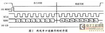
The serial communication cycle of the AD9852 is divided into two phases. The first eight rising edges of SCLK correspond to the instruction cycle. In the instruction cycle, the user sends a command word to the serial controller of the AD9852 to control the subsequent serial data transmission. The data transfer cycle starts from the 9th rising edge of SCLK, the input data is written on the rising edge of the clock, and the output data is read on the falling edge of the clock. The data transmitted by the serial port is first written into the I/O buffer register. When the system receives a valid update signal, it writes these data into the internal control register set and completes the corresponding functions. When the communication cycle is completed, the AD9852 serial controller assumes that the rising edge of the next eight system clocks corresponds to the instruction word of the next communication cycle.
When a high input is present on the I/OSE SET pin, the current communication cycle will be terminated immediately. When the I/O RESET pin returns to a low level, the AD9852 serial port controller considers the next eight system clocks to rise. Along the instruction word that corresponds to the next communication cycle, this is very useful for keeping the synchronization of the communication.
4, 2 AD9852 synchronous work to achieve two AD9852 output signal waveform phase synchronization is the key to make them work in the same system clock, the phase error between each AD9852 system clock can not exceed one cycle. The system clock of the AD9852 can be supplied directly from the reference clock, or the reference clock can be amplified by an internal clock multiplier. The asynchronous update clock is synchronized with the system clock after passing through the edge detection circuit inside the AD9852, forming a rising edge and triggering an update of the internal control register. Therefore, to achieve the synchronization of two AD9852s, it is necessary to synchronize the reference clock with the rising edge of the update signal. The following are some important points to ensure that the two AD9852s work synchronously.
4.1 Reference clock signal The AD9852 reference clock has two types of differential input and single-ended input. Since the differential clock has shorter rise and fall times on the pulse edge and the minimum jitter rate, it can effectively reduce the two AD9852 reference clock Phase error, so the system uses a reference signal differential input. For the differential input method, the input signal can be a square wave or a sine wave. It is recommended to use the MAX9371 from MAXIM, which can convert ordinary clock signals into the differential clock signals required by the system. In order to achieve the reference clock synchronization, so that two AD9852 use a crystal, crystal output signals are first passed to the two differential clock generators, after conversion input 2 AD9852. In order to make the delay time of each AD9852 reference clock signal consistent in the transmission process, PCB wiring must ensure that the clock signal trace distance is the same.
4.2 Updating Clock Signals When programming the AD9852, serial input data is buffered in the internal I/O buffer register and does not affect the working state of the AD9852. After the rising edge of the update clock signal arrives, the I/O is triggered. The O buffer register transfers data to the internal control register, which can complete the corresponding function and control the output signal. There are two ways to update the clock signal, one is generated automatically by the AD9852 chip, the user can program the frequency of the update clock to generate a fixed period internal update clock, and the other is provided by the user to provide an external update clock. The AD9852I/OUD pin is an input pin that is signaled by an external controller. In order to achieve the synchronization of two AD9852s, it is necessary to ensure that the rising edge of their updated clock signal comes at the same time, so the system adopts an external clock update method. Using an I/O port of the DSP to connect to the I/OUD of the AD9852, software can accurately control the rising edge of the updated clock signal. The wiring requirements for externally updated clock signals are the same as for reference clocks.
4.3 Reference Clock Doubler The AD9852's operating clock is as high as 300MHz. To reduce the interference of the clock signal, the system should use a low-frequency clock signal source, and then use the AD9852 on-chip reference clock multiplier to implement an external reference clock of 4 to 20 times the frequency. . The phase-locked loop circuit of the reference clock doubler has two working states: a locked state and a locked state. In the locked state, the system clock signal and the reference clock signal can remain synchronized. However, when sending a control instruction to the AD9852, the PLL cannot lock immediately after the reference clock doubler operates, and still operates to obtain the locked state. At this time, the number of system clock cycles sent to the AD9852 phase accumulator is uncontrollable. This may cause phase out of synchronization between the output signals of the two AD9852s. Therefore, after the system is initialized, it is necessary to ensure that the phase-locked loop enters the lock first. Status before the various control words inside the AD9852 can be updated. The typical time for locking the AD9852 on-chip PLL is approximately 400μs. It is recommended to leave at least 1ms for the PLL to enter the locked state.
5, AD9852 control flow (1) to the system power, issued by the DSP to the AD9852 reset signal, this signal needs to maintain at least 10 reference clock cycles high.
(2) Set S/PSELECT to 0 to select the serial data input method.
(3) Each control word is sent to each AD9852 in turn, so that each AD9852 operating state is changed from the default internal update clock mode to an external clock update mode.
(4) Write the control word of AD9852 clock frequency multiplier work into each I/O buffer register of AD9852 in turn, then send out the external update clock by DSP, update each AD9852 internal control register.
(5) The DSP issues an external update signal, waiting for at least 1.0ms to lock the AD9852's internal phase-locked loop. Then DSP sends relevant signal waveform parameter to AD9852, carries on the synchronous update to their internal control register content, causes 2 pieces of AD9852 outputs the synchronous simulation signal.
6. Conclusion Using the DSP to control the knock signal and Camshaft signal generated by the AD9852, both the accuracy and real-time performance can meet the hardware-in-the-loop simulation requirements of the engine electronic control unit. On the basis of this system, it can be further extended to use synchronously for multiple pieces of DDS, and it is applicable to more hardware-in-the-loop simulation systems.
Hydraulic Valve,Hydraulic Pressure Relief Valve ,Hydraulic Relief Valve ,Small Hydraulic Pump
Engineering & Construction Machinery Parts Co., Ltd. , http://www.nbengineparts.com